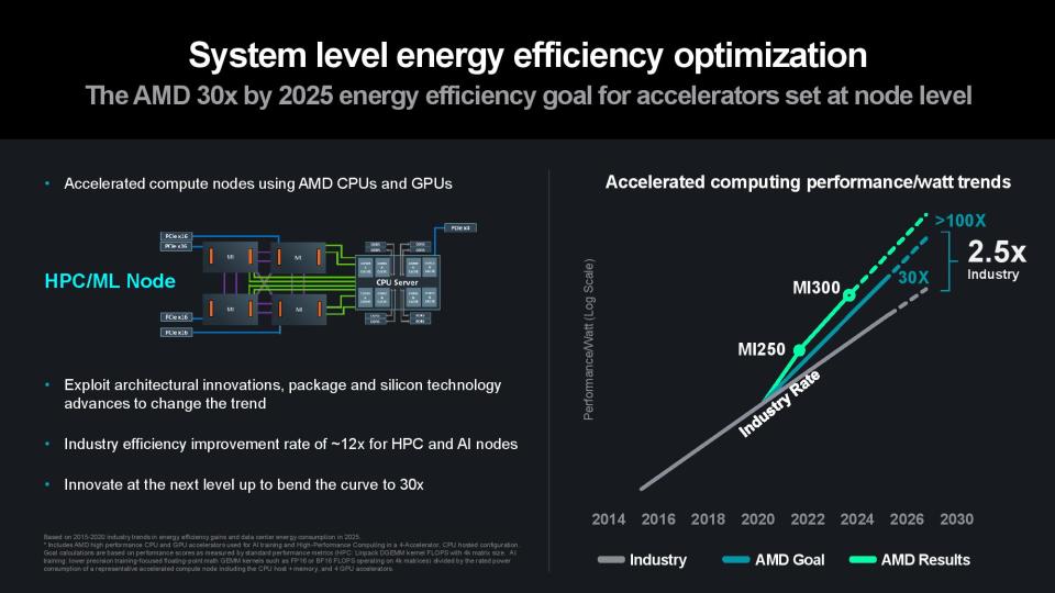
AMD CEO Lisa Su attended imec’s ITF World 2024 conference to accept the prestigious imec Innovation Award for innovation and industry leadership, joining the ranks of other previous honorees like Gordon Moore, Morris Chang, and Bill Gates. After accepting the award, Su launched into her presentation covering the steps that AMD has taken to meet the company’s 30×25 goal, which aims for a 30x increase in compute node power efficiency by 2025. Su announced that AMD is not only on track to meet that goal, but it also now sees a pathway to more than a 100x improvement by 2026 to 2027.
Concerns about AI power usage have been thrust into the limelight due to the explosion of generative AI LLMs like ChatGPT, but AMD had the vision to foresee problems with AI’s voracious power appetite as far back as 2021. Back then, AMD began work on its 30×25 goal to improve data center compute node power efficiency, specifically citing AI and HPC power consumption as a looming problem. (AMD set its first ambitious energy goal back in 2014 with its inaugural 25×20 goal to improve consumer processor power efficiency by 25x by 2020, which it exceeded with a 31.7x improvement.)
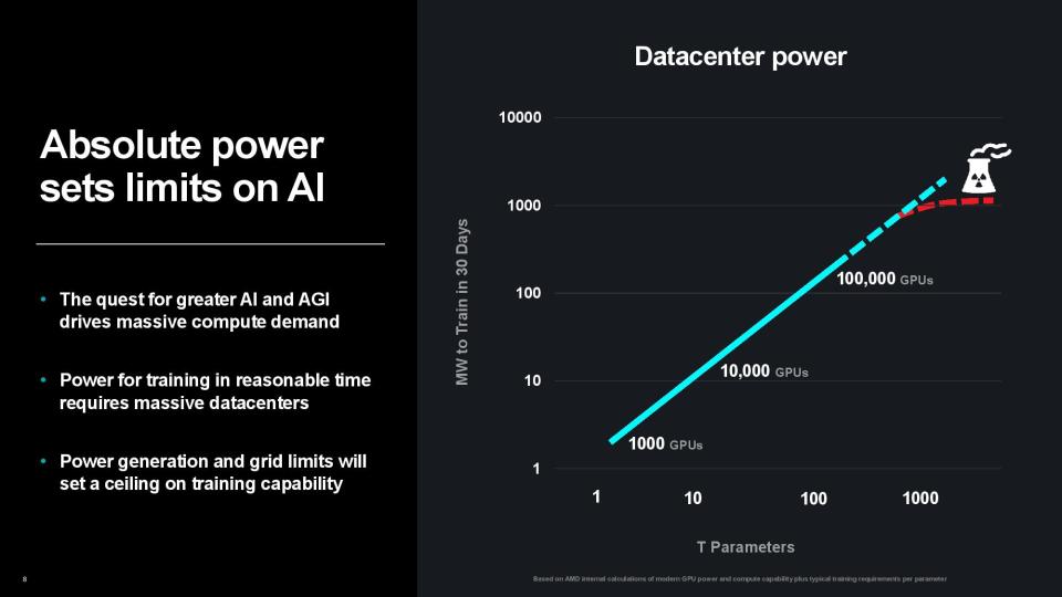

That problem has now come to the forefront. Generative AI is fueling the rapid expansion of data centers as the world’s largest companies vie for AI supremacy, but public power grids aren’t prepared for a sudden surge of power-hungry data centers, making power the new limiting factor. There are hard limits on the amount of power available to data centers as grid capacity, infrastructure, and environmental concerns limit the capacity that can be dedicated to both new and expanding data centers alike. In fact, many new data centers are being constructed next to power plants to ensure the supply of power, and the crushing demand has even reignited the push for nuclear Small Module Reactors (SMRs) to supply individual data centers.
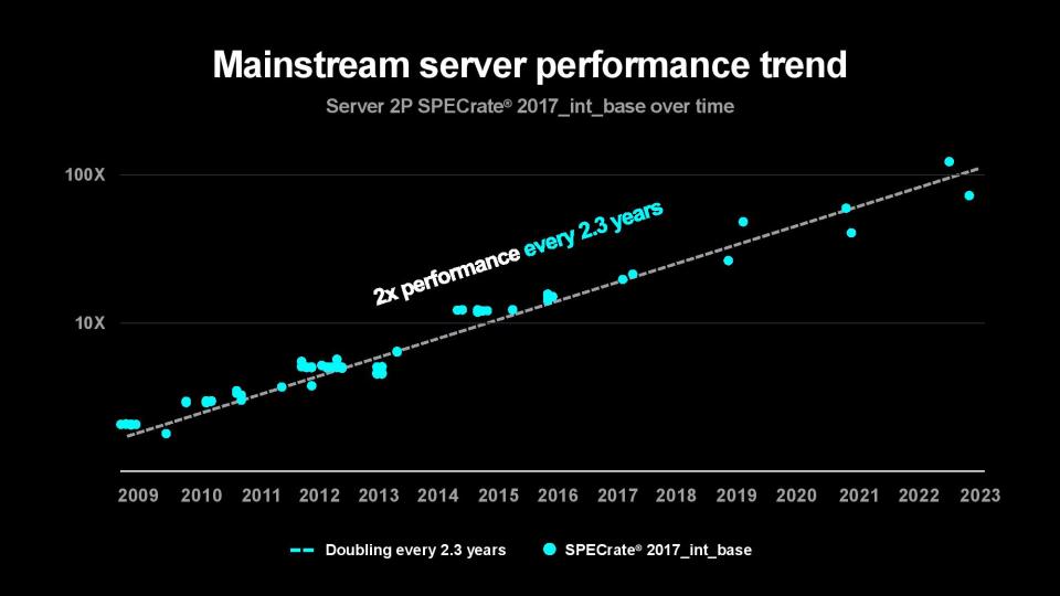

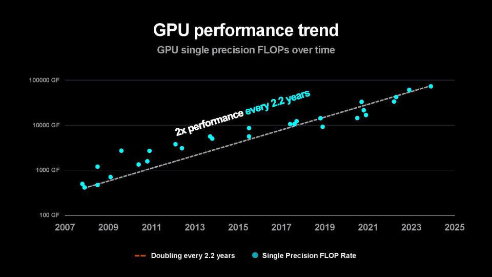

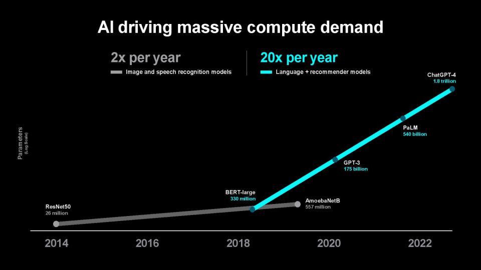

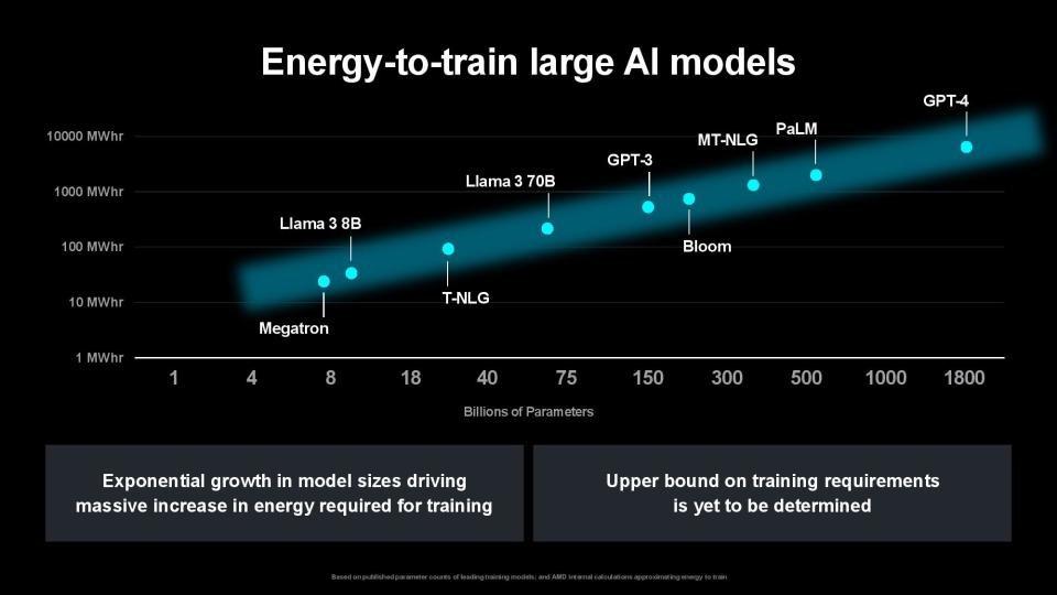

The problem is only intensifying as the compute required to train models increases. Su pointed out that the size of the first image and speech recognition AI models used to double every two years, largely matching the pace of advances in computing power over the last decade. The size of generative AI models is now growing at 20x per year, however, outstripping the pace of computing and memory advancements. Su said that while today’s largest models are trained on tens of thousands of GPUs consuming up to tens of thousands of megawatt-hours, rapidly expanding model sizes could soon require up to hundreds of thousands of GPUs for training, perhaps requiring several gigawatts of power to train a single model. That clearly isn’t tenable.
AMD has a multi-pronged strategy for improving power efficiency, consisting of a broad approach that expands beyond its silicon architectures and advanced packaging strategies to AI-specific architectures, system- and data center-level tuning, and software and hardware co-design initiatives.
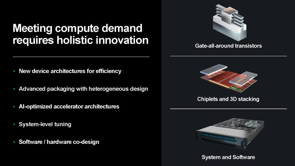

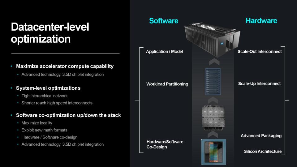

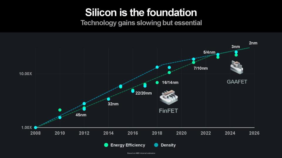

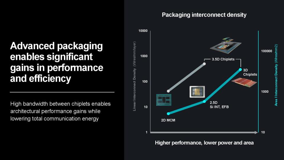


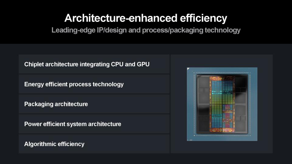


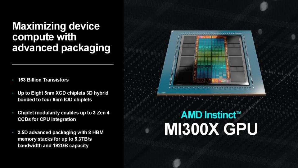

Naturally, silicon is the bedrock. Su pointed to 3nm Gate All Around (GAA) transistors as AMD’s next step on the silicon roadmap to improve power efficiency and performance, along with a continued focus on advanced packaging and interconnects that enable more power-efficient and cost-effective modular designs. Advanced packaging plays a key role in scaling out designs to produce more horsepower within the constraints of a single chip package, and AMD employs a mix of 2.5D and 3D packaging to maximize the amount of compute-per-watt it can wring from each square millimeter of data center silicon.
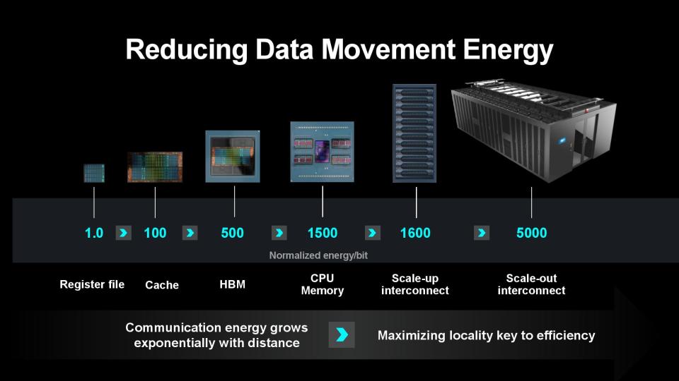
Transferring data between server nodes and server racks consumes extra power due to longer distances, so optimizing for data locality can yield tremendous power savings. AMD’s MI300X is a great example of the efficiency wrung from making ever-larger chip packages — the chip wields 153 billion transistors spread across 12 chiplets paired with 24 HBM3 chips that provide 192GB of memory capacity, all of which is available to the GPU as local memory. Paired with power- and performance-optimized infinity Fabric interconnects between the in-package units, the extreme compute and memory density keeps more data close to the processing cores, thus reducing the amount of energy required to transfer data.
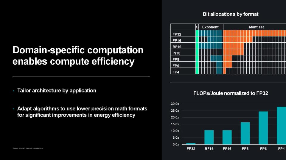


Su said that while hardware optimizations are important, AMD’s work on hardware and software co-optimization also yields impressive results. Using lower-precision numerical formats boosts power efficiency and performance, so designing in specific hardware acceleration is important for continued scaling. As you can see in the slides above, moving to lower-precision formats like FP4 drastically increases the FLOPs per Joule of consumed energy – compared to FP32, FP8 delivers a 15x increase in power efficiency while FP4 delivers around a 30x improvement.
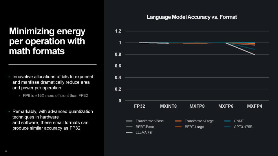
Lower precision results in lower accuracy, but Su highlighted that advanced quantization techniques have helped address that issue. In fact, even MXFP6 can produce similar accuracy to FP32, with a drop off only seen at MXFP4 with a few of the different models, while others are still just as accurate. Work continues on improving the accuracy of low precision formats, so we could even see MXFP4 become just as accurate as FP32 across many more models in the future.
Overall, Su said that AMD has exceeded the industry’s rate of progress on power efficiency per node as the company remains on pace to meet its 30x power efficiency improvement. Su expects that trend to continue, saying, “With this type of innovation, based on what we see today, we think we can do better than that. We are on track to do greater than 100 times by the time we get up to 2026 and 2027. And there’s much, much more we can do in this area.”
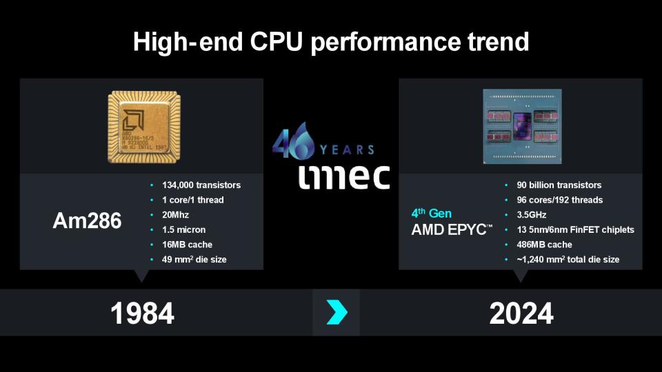



Imec’s event had a strong roster of presenters from multiple semiconductor companies, like ASML, TSMC, Intel and SK hynix, among others, and many of the speakers echoed Su’s sentiments that data center power consumption, and the environmental ramifications associated with it, are becoming a first-order problem.
Su noted that continuing the pace of power efficiency improvements will take an industry-wide effort. “We have the opportunity to drive that ecosystem by bringing many different capabilities and many different expertise’s together. I think that’s the key for the next generation of innovation,” Su said.
“We’re all experts in certain areas, but when we bring process folks, packaging folks, hardware designers, architects, software’s models and systems designers together, we can get that holistic design capability that really bend the curve of innovation going forward,” Su said.
Producing processors is also a carbon and water-intensive process, so sustainability was a key topic at the event. Su didn’t touch on the company’s progress in reducing its carbon footprint, but the company recently outlined its achievements in that area in a blog post, saying that leveraging chiplet-based architectures has saved ~50K metric tons of CO2e in 2023 simply by yield improvements that ultimately reduce the number of wafers it needs to fab. That single year’s C02e savings was equivalent to AMD’s entire operational footprint for the entire year of 2022, highlighting that AMD is tackling environmental challenges from multiple angles.
Source Agencies

